|
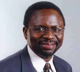
Ilesanmi Adesida
birth: ; place:
.education.gif) B.S.
electrical engineering (1974) the University of California, Berkeley;
M.S. electrical engineering (1975) the University of California,
Berkeley B.S.
electrical engineering (1974) the University of California, Berkeley;
M.S. electrical engineering (1975) the University of California,
Berkeley
 Ph.D.
electrical engineering (1979) University of California, Berkeley Ph.D.
electrical engineering (1979) University of California, Berkeley
|

|
|
 professor in the
U of I Department of Electrical and Computer Engineering, an
affiliate faculty member in the Beckman Institute Nanoelectronics
and Biophotonics group, and the director of the U of I Microelectronics
laboratory professor in the
U of I Department of Electrical and Computer Engineering, an
affiliate faculty member in the Beckman Institute Nanoelectronics
and Biophotonics group, and the director of the U of I Microelectronics
laboratory
URL: http://www.beckman.uiuc.edu/profiles/faculty/iadesida.html
|
From 1979 to 1984, Dr. Adesida worked in various capacities
at what is now known as the Cornell Nanofabrication Facility and
the School of Electrical Engineering, Cornell University, Ithaca,
NY. He was the Head of the Electrical Engineering Department at
Tafawa Balewa University, Bauchi, Nigeria, from 1985 to 1987.
He then joined the University of Illinois at Urbana-Champaign,
where he is currently the Donald Biggar Willet Professor of Engineering,
Professor of Electrical and Computer Engineering, Professor of
Materials Science and Engineering, the Director of the Micro &
Nanotechnology Laboratory, and the Director of the Center for
Nanoscale Science and Technology. He has also previously served
as the Associate Director for Education of the NSF Engineering
Research Center for Compound Semiconductor Microelectronics from
1990 to 1997. In collaboration with colleagues, his efforts led
to the award of the NSF Nanoscale Center for Chemical-Electrical-Mechanical-Manufacturing
Systems to the University of Illinois in 2003. His research interests
include nanofabrication processes and ultra-high-speed optoelectronics.
He has extensive experience in the development of novel processes
for wide bandgap materials such as silicon carbide and gallium
nitride. He has also worked on ultra-high-speed photodetectors
and photoreceivers in various materials systems. Professor Adesida
has chaired many international conferences including serving as
the Program and General Chair of the Electronic Materials Conference
from 2000 to 2003. He is a Fellow of the Institute of Electrical
and Electronic Engineers (IEEE), the American Association for
the Advancement of Science (AAAS), and the American Vacuum Society
(AVS). He is serving as the President-Elect of the IEEE Electron
Device Society in 2004 and 2005.
Honors: Associate, UIUC Center for Advanced Study; Vice-chair,
Electronic Materials Committee; Fellow, IEEE (1999); Oakley-Kunde
Award for Excellence in Undergraduate Education; University Scholar;
Best Paper Award, International Conference on Micro- and Nano-Engineering
(1996); Fellow, IEEE; IEEE EDS Distinguished Lecturer; UIUC College
of Engineering's List for Advising Excellence; Member, Bohmische
Society; EMSA Presidential Student Award.
RESEARCH
Professor Adesida's fields of interest are
advanced materials processing and high speed semiconductor optoelectronic
devices and circuits. He conducts research on nanostructures,
semiconductor processing, and devices. He has collaborated with
Professor P. Bohn in fabricating nanometer scale gold probes to
detect single molecules via resistively-monitored thiol chemisorption.
His other activities center on studying dislocations in GaN using
photoelectrochemical etching and investigating ultra-high speed
field-effect transistors in various hererostructures such as AlGaN/GaN,
GaAs/InGaAs, and SiGe/Si.
He has 253 journal papers of which many are
in the Journal of Applied Physics and Applied Physics Letters;
186 conferences papers, 23 supervised Ph.D students...More on
his publications list and at: http://www.ece.uiuc.edu/faculty/faculty.asp?iadesida
and http://www.micro.uiuc.edu/apc/AdePublications.pdf.
Recent, Representative Publications
Farid, K. A., Zhou, L., Ping, A. T., and Adesida, I. (1999),
"ICP-RIE Etching of AlxGa1-xN for Applications in Laser Facet
Formation," Journal of Vacuum Science and Technology, B17,
pp. 2750-2754.
Farid, K. A. and Adesida, I. (1999), "High Rate Etching
of SiC Using Inductively Coupled Plasma Reactive Ion Etching in
SF6-based Gas Mixtures," Applied Physics Letters, 75, pp.
2268-2270.
Dumka, D. C., Cueva, G., Adesida, I., Hier, H. and Aina, O.
A. (1999), "Doped Multichannel AlAs0.56Sb0.44/In0.53Ga0.47As
Field Effect Transistors," Electronics Letters, 35, pp. 1673-1674.
Adesida, I., Mahajan, A., Cueva, G., and Fay, P. (1999), "Novel
HEMT Processing Technologies and Their Circuit Applications,"
Solid State Electronics, 43, pp. 1333-1338.
Ping, A. T., Selvanathan, D., Youtsey, C., Adesida, I., Piner,
E., and Redwing, J. (1999), "Gate Recessing of GaN MESFETs
Using Photoelectrochemical Wet Etching," Electronics Letters,
35, pp. 2140-2141.
Youtsey, C., Romano, L. T., Molnar, R. J., and Adesida, I.
(1999), "Rapid Evaluation of Dislocation Densities in n-type
GaN Films Using Photoenhanced Etching," Applied Physics Letters,
74, pp. 3537-3539.
references: R. Guibinga; http://www.beckman.uiuc.edu/profiles/faculty/iadesida.html;

![]() B.S.
electrical engineering (1974) the University of California, Berkeley;
M.S. electrical engineering (1975) the University of California,
Berkeley
B.S.
electrical engineering (1974) the University of California, Berkeley;
M.S. electrical engineering (1975) the University of California,
Berkeley![]() Ph.D.
electrical engineering (1979) University of California, Berkeley
Ph.D.
electrical engineering (1979) University of California, Berkeley

![]() professor in the
U of I Department of Electrical and Computer Engineering, an
affiliate faculty member in the Beckman Institute Nanoelectronics
and Biophotonics group, and the director of the U of I Microelectronics
laboratory
professor in the
U of I Department of Electrical and Computer Engineering, an
affiliate faculty member in the Beckman Institute Nanoelectronics
and Biophotonics group, and the director of the U of I Microelectronics
laboratory